In the field of science and research, University of Žilina (UNIZA) participates in 200 national and 41 international scientific projects and organizes about 60 scientific and professional events annually. There were two new significant workplaces established within the Operational Programme Research and Development in 2013 – University Science Park and Research Centre. Results of science and research activities of the University have an important influence not only on the educational activities but also on the development of international cooperation or interconnection with practice.
The cooperation with foreign universities and institutions is crucial for UNIZA. UNIZA has signed bilateral cooperation agreements with more than 150 foreign partners, and it belongs to the most successful universities within the Erasmus Programme, both in the number of seconded staff and students.
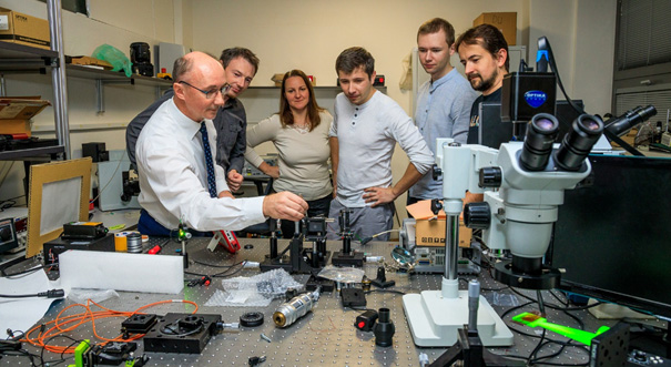
The Department of Physics in Faculty of Electrical Engineering and Information Technology provides basic physics courses for all UNIZA faculties. The Department is focused on the development and application of optic and photonic elements on a chip, optic fibers, application of acoustic wave processes on condensed matter and theoretical studies of elementary particles.
The section of Optics and Photonics is a team of young researchers that aims its activities in study, preparation, and analysis of photonic structures. First team studies physical properties of the special optical fibers such as capillary and photonic fibers, and photonic sensors. The latest results are in the area of sensors on a chip, and fibers for the laboratory on a chip. Second team has extended its activities to laser technologies by preparation and analysis of photonic structures for integrated optics and optoelectronics. The cutting-edge photonic elements for applications on a chip and optic fibers are developed using 3D laser lithography in submicrometer scale. In the field of active devices, the new types of light emitting diodes with patterned surface using photonic structures and polymeric membranes with photonic structure were developed.
Our experiences with laser 3D patterning started app. from y. 2006, where Ar ion laser 488 nm was firstly used for fabrication of 1D and 2D gratings in thin photoresist layer. In the next years, we were focused on fabrication and integration of gratings on optoelectronic devices and sensors. Significant results were obtained in plasmonics as well, where plasmonic sensors based on 2D gratings, and 3D substrates for Surface-enhanced Raman spectroscopy were produced. Latest results are focused on 3D laser lithography using polymer IP-Dip and 3D micropatterning and microprinting in submicrometer resolution down to 100 nm.